The Contact Problem in 2D Semiconductors
Two-dimensional semiconductors, such as transition metal dichalcogenides, have long promised a future of ultra-thin, flexible, and energy-efficient electronics. Their atomically thin nature enables superb electrostatic control, making them attractive candidates to extend Moore's law beyond conventional silicon. Yet one stubborn obstacle has stood in the way of practical devices: forming reliable, low-resistance metal contacts.
Because 2D channels are only a few atoms thick, the interface between the metal electrode and the semiconducting channel dominates device performance. Poor contact quality leads to large contact resistance, heat dissipation, and degraded switching characteristics. Traditional metal deposition methods often damage the delicate lattice, introduce disorder, or create Schottky barriers that block charge injection.
Researchers have tried numerous strategies, from van der Waals lamination to phase engineering, but many require complex transfer processes or produce contacts that are not stable at scale. A new study reported in Science, Volume 393, Issue 6814, presents an approach that could sidestep these hurdles: direct evaporation of single-crystal metal contacts onto 2D semiconductors.
What the Study Reports
The paper, titled “Direct evaporation of single-crystal metal contacts for 2D semiconductors,” demonstrates a method to form metal contacts that are themselves single-crystalline, directly on the surface of a 2D semiconductor. Published in the August 2026 issue of Science, the work tackles the contact problem by controlling the metal's crystal structure during deposition.
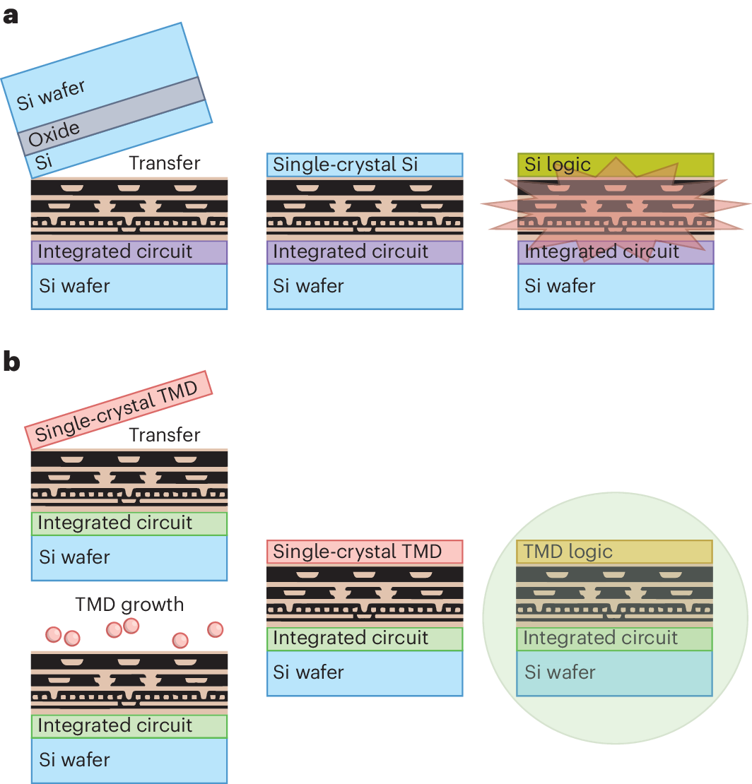
Rather than relying on polycrystalline metal films, which contain grain boundaries that scatter carriers and create uneven interfaces, the researchers evaporate metal atoms in a way that allows them to assemble into a single crystal over the 2D lattice. This creates an abrupt, clean, and structurally coherent interface with potentially near-ideal electronic properties.
The Role of Epitaxy
The key insight lies in epitaxial growth. Under carefully chosen conditions, the evaporated metal atoms can align with the crystal lattice of the underlying 2D semiconductor. The resulting single-crystal contact is atomically matched, reducing interfacial states and suppressing Fermi-level pinning. This is a significant departure from conventional evaporation, which typically yields randomly oriented polycrystalline grains.
By directly evaporating the metal, the method avoids the need for lithography steps that expose the 2D material to solvents and resists, preserving its intrinsic quality. It also opens a path toward wafer-scale fabrication, since evaporation is compatible with standard semiconductor processing lines.

Why Single-Crystal Contacts Matter
In today's electronic devices, metal contacts are everywhere from transistors to interconnects. For 2D materials to become viable, contacts must meet several criteria:
- Low contact resistance to enable fast switching and low power consumption
- Thermal stability to withstand processing and operation
- Uniformity across a wafer so that millions of devices behave identically
- A clean interface with minimal chemical disorder or contamination
Polycrystalline contacts fail on uniformity and often increase resistance due to grain-boundary scattering. Single-crystal contacts, by contrast, offer a perfectly ordered interface. They can also help to align work functions more predictably, reducing the Schottky barrier height. This is particularly important for n-type and p-type 2D semiconductors, where contact engineering controls whether electrons or holes can be injected efficiently.
The technique described in the Science paper could therefore be a crucial step toward high-performance 2D transistors, photodetectors, and sensors.
Implications for Next-Generation Electronics
If the method scales beyond the laboratory, it could accelerate development of 2D-material-based logic circuits. The semiconductor industry has been exploring 2D channels for years as a post-silicon option for sub-1 nanometer nodes. But contact resistance has been repeatedly cited as a major bottleneck. A direct evaporation approach that yields single-crystal contacts without complex transfer processes is a compelling candidate for industrial adoption.
Furthermore, single-crystal metal contacts may also benefit emerging device architectures such as field-effect transistors with 2D channels and vertical heterojunctions. The ability to deposit crystals of different metals could allow selective contact doping or even the formation of atomically sharp metal-semiconductor junctions with engineered band alignments.

Open Questions and Future Directions
While the title of the paper clearly demonstrates the concept, many details about the generalizability of the technique will be eagerly examined by the community. How many metal-semiconductor combinations are compatible with this approach? What are the exact deposition conditions, and can they be controlled with enough precision for production?
It is also not yet clear whether the single-crystal contacts retain their structure after subsequent processing steps such as annealing or encapsulation. Researchers will likely explore these aspects in follow-up studies. The fact that this work appears in such a prominent journal as Science underscores its potential importance and the expectation that it will inspire further innovation.
The Road Ahead
For decades, silicon technology has been perfected through incremental improvements. Moving to 2D semiconductors will require a fundamental rethinking of device contacts, materials, and processes. The direct evaporation of single-crystal metal contacts provides a fresh path forward — one that leans on established semiconductor manufacturing tools while embracing the unique atomic-scale needs of 2D materials.
As researchers continue to refine the technique and probe its limits, the semiconductor community will be watching closely. If the promise holds, this advance could help bring 2D semiconductors from the research lab to the fab floor, enabling the next leap in electronics.
The study appears in Science, Volume 393, Issue 6814, a peer-reviewed venue known for highlighting breakthrough discoveries. Its arrival signals that contact engineering remains one of the most active and critical areas in materials science, and that direct evaporation of single-crystal contacts could be a lasting contribution.
This article is based on reporting by Science (AAAS). Read the original article.

Originally published on science.org