A printed circuit board is flat because flat is convenient. It is easy to screen-print, easy to populate with components and easy to slot into a housing. Real objects are rarely so cooperative. Device enclosures curve, helmets taper, aircraft skins bend, and medical devices must follow anatomy that no rectangular substrate can match. A new mist-based printing method, described as a way to build electronic circuits directly onto curved and three-dimensional surfaces, is aimed squarely at that mismatch.
The appeal is not decorative circuitry on novelty shapes. It is the prospect of turning the surface of an object into the circuit itself — depositing wiring, sensors and antennas onto geometry that already exists, rather than designing a product around the flat board that has to fit inside it.
How mist-based deposition works
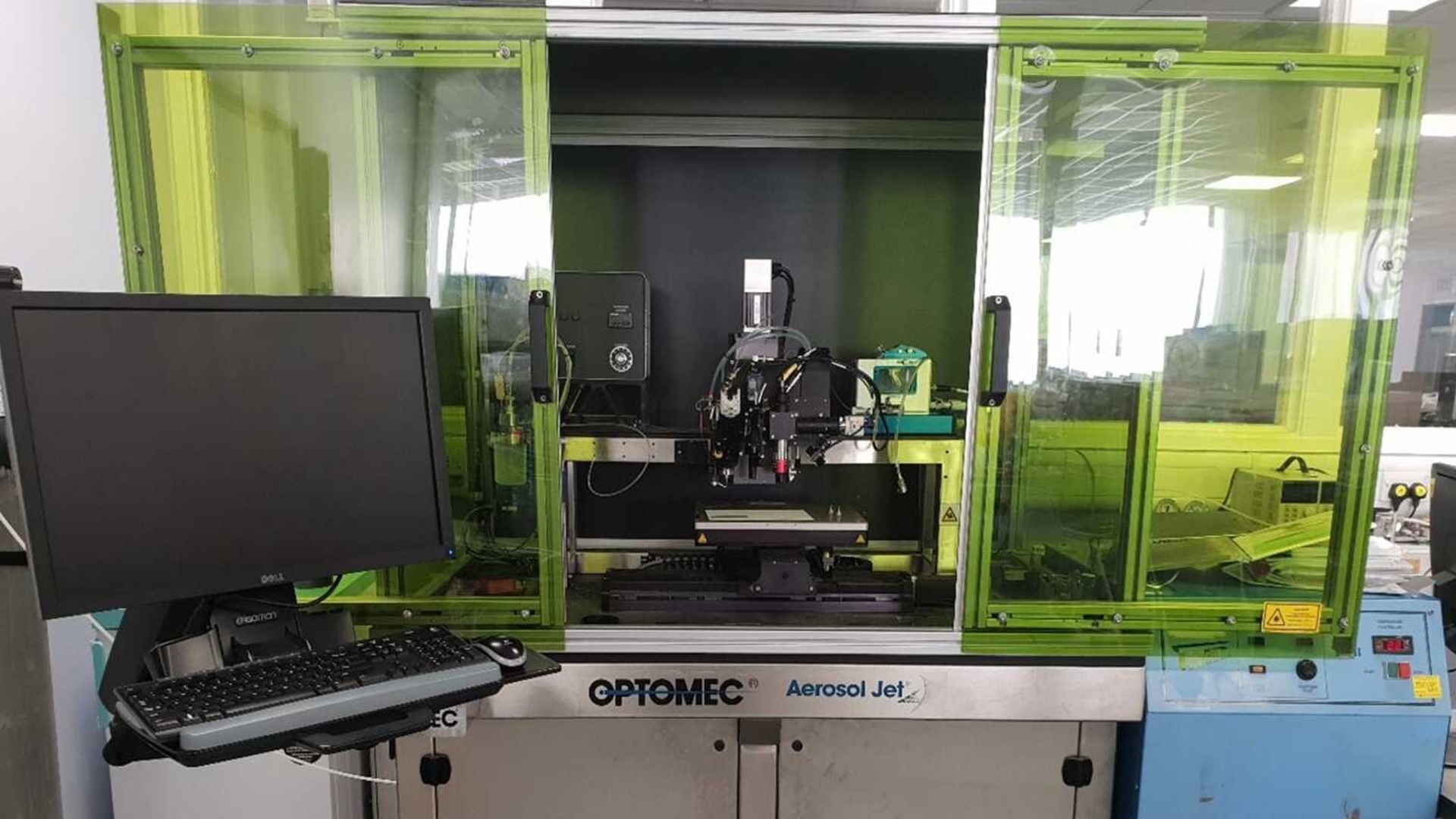
Instead of pressing ink through a screen or extruding it as a continuous bead, mist-based approaches start with a liquid ink that is broken into an extremely fine aerosol. The result is closer to a controlled fog than a jet of liquid: a cloud of microscopic droplets suspended in a carrier gas.
That aerosol is then guided through a deposition head, where the flow is shaped and accelerated. Because the droplets are so small and the stream can be focused aerodynamically, the material can be aimed at a surface from a standoff distance rather than pressed against it. That standoff is the key to curved and stepped geometry. The print head can follow a contour without touching it, and the surface beneath does not have to be flat.
From droplets to solid traces
Once the mist lands, the droplets coalesce into a thin wet line. A curing or sintering step — usually heat, sometimes light — then drives off solvent and fuses the material into a conductive path. Because deposition and consolidation are separate stages, the process can be tuned. Additional passes build thicker, lower-resistance lines; fewer passes produce finer features. The same flexibility allows a pattern to be laid down across a surface that changes angle mid-pass.
The multi-material opening
Because the material arrives as an aerosol rather than as a fixed filament or a screen-defined stencil, a single tool can in principle switch between inks. A conductive metal forms the wiring, a dielectric provides insulation between layers, and a resistive or piezoresistive paste becomes a sensing element. Stacking those layers yields more than wiring on a curve: it yields antennas, capacitors, strain gauges and electrodes built up from the surface itself.

The geometry problem it addresses
Conventional printing struggles with curvature for reasons that are geometric before they are chemical. Screen printing relies on a flat, tensioned mesh pressed against the substrate; wrap that mesh around a cylinder and registration and tension both degrade. Inkjet and extrusion methods need a controlled gap between nozzle and surface, and on a curved part that gap changes constantly — which changes line width, thickness and electrical resistance along the same trace. Add steps, recesses or compound curvature, and maintaining a constant working distance becomes a motion-control challenge as much as a materials one.

A non-contact mist process relaxes that constraint, though it does not eliminate it. Deposit quality still depends on the distance and angle between head and surface, and deeply recessed or shadowed regions remain difficult to reach reliably.
Where the approach could be applied
- Aerospace and defense: antennas, sensors and heating elements printed onto curved panels, radomes and interior structures, avoiding the weight and fastener count that comes with mounting separate boards.
- Wearables: electrodes and interconnects deposited onto textiles or flexible bands that flex with the body rather than resisting it.
- Medical devices: sensor arrays on catheters, prosthetics and surgical instruments, where shape is dictated by anatomy rather than by manufacturing convenience.
- Automotive and industrial: strain and temperature sensors placed on curved structural components, or heating elements spread across a shaped surface.
- Consumer electronics: antennas and touch-sensing layers integrated into curved casings and displays.

What still has to be solved
The obstacles between a promising deposition method and volume manufacturing are practical and numerous. Adhesion is the first: a trace must survive flexing, thermal cycling and handling on a substrate that may be metal, composite, polymer or ceramic.
Thermal budget is the second. Sintering metallic inks often requires temperatures that many plastics, composites and finished assemblies cannot tolerate, so the curing step may need to be localized, shortened or reformulated to protect the underlying part.
Then there is the classic tension between resolution and throughput. Fine features and thick conductive layers pull in opposite directions, and multi-pass deposition takes time. Yield and inspection on non-planar surfaces are harder still: optical inspection systems are built around flat fields of view, and measuring a trace that wraps around a curve is not a solved problem.
Finally, printed conductors rarely replace every component. Chips, connectors and power components still need to be attached, which means the industry also needs pick-and-place and joining techniques that work on curved, populated surfaces.
A smaller boundary between structure and circuit
Flat boards will not disappear. They are cheap, well understood and supported by an enormous manufacturing ecosystem. But the line between the object and its electronics is softening. If circuits can be deposited onto the shapes that engineering and anatomy already demand, designers gain a new degree of freedom: instead of asking how to fit a board into a product, they can ask which parts of the product should simply become the board.
The mist-based method is one route toward that outcome, and its most interesting property may be the least glamorous one — it does not need the surface to be flat.
This article is based on reporting by Interesting Engineering. Read the original article.

Originally published on interestingengineering.com