Silicon photonics has long promised to bring the speed of light to computing and communications, but the technology has been dogged by a stubborn problem: light that bounces back. Now, Kyocera and Tohoku University say they have demonstrated a world-first laser method that reduces back-reflected light by 95% on silicon photonics chips. The development, reported by Interesting Engineering, could help solve a growing bottleneck for integrated optical systems.
Why back-reflected light matters
In a photonic integrated circuit, light travels through waveguides, splitters, modulators, and other components. At every interface where the refractive index changes, a fraction of the light can reflect backward. These reflections may seem minor, but they can return to the laser source and disrupt its operation. The result can be increased noise, unstable output power, mode hopping, and reduced signal integrity.
For decades, engineers have relied on optical isolators to block this backward-traveling light. An isolator acts like a one-way valve for photons: it lets light pass in the forward direction while absorbing or diverting light that tries to go backward. Without isolation, many laser-based systems simply cannot operate reliably.

The challenge of integrating isolators
Traditional optical isolators are bulky and difficult to integrate on a silicon chip. They often depend on magneto-optic materials, such as garnets, and require precise magnetic fields. Depositing these materials on silicon without degrading optical performance is complex and expensive. As a result, many silicon photonics systems still use external isolators, which undermines the goal of compact, low-cost integrated photonics.
That is why the new result from Kyocera and Tohoku University is attracting attention. Instead of relying on conventional isolator materials, the team used a laser-based method to cut back-reflected light by 95%. The approach is described as a world first, and it points to a potentially simpler path toward managing reflections directly on silicon photonics chips.
What the 95% reduction means
A 95% reduction in back-reflected light is a substantial improvement. In optical systems, even small amounts of feedback can cause problems, so suppressing the majority of reflections can significantly improve laser stability and signal quality. The remaining 5% may still require careful management, but the achievement suggests that on-chip reflection control is becoming more feasible.
According to the report, the technology could help address a growing challenge: as silicon photonics moves from laboratory demonstrations to commercial products, the demands on optical performance are increasing. Data centers, AI accelerators, and high-speed interconnects need ever more bandwidth with lower power consumption. Reflections that were tolerable in early prototypes can become serious obstacles at scale.

Kyocera and Tohoku University collaboration
The work combines Kyocera’s expertise in materials and manufacturing with Tohoku University’s research capabilities in photonics and laser science. Japan has a long history of leadership in optical technologies, and collaborations between industry and academia are increasingly important for moving innovations from the lab to the fab.
While the full technical details have not been widely disclosed in the initial report, the collaboration signals that the method is being developed with practical integration in mind. Kyocera’s involvement suggests a focus on manufacturability, reliability, and scalability—factors that often determine whether a laboratory breakthrough becomes a commercial technology.

Silicon photonics at a turning point
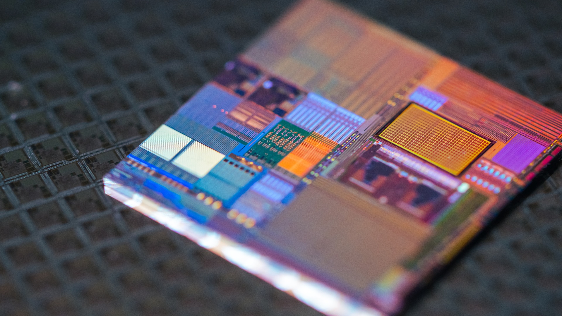
Silicon photonics uses silicon-based waveguides and components to manipulate light. Because it leverages established semiconductor manufacturing, it can potentially produce optical devices at high volume and low cost. The technology is already used in transceivers for data centers, and it is being explored for LiDAR, biosensing, quantum computing, and optical interconnects between chips.
One of the biggest roadblocks has been the lack of a practical, integrable optical isolator. If the Kyocera–Tohoku laser method can be scaled and standardized, it could remove a key limitation. That would allow designers to pack more photonic functions onto a single chip without worrying as much about feedback-induced instability.

Remaining questions and next steps
Any new technology faces questions before widespread adoption. Researchers will need to demonstrate that the 95% reduction holds across different wavelengths, temperatures, and manufacturing tolerances. They will also need to show that the laser method is compatible with high-volume fabrication and does not introduce excessive losses in the forward direction.
- Can the method be reproduced consistently in commercial foundries?
- How does it perform over the lifetime of a device?
- Does it add significant cost or complexity to existing process flows?
- Can it be combined with other on-chip photonic components without interference?
These questions are typical for any emerging photonic technology, but the early result is promising. A 95% reduction is a strong starting point, and it may spur further research into laser-based reflection control.
Potential applications
If the approach proves viable, it could benefit a wide range of systems. Data center interconnects could become more efficient and reliable. Optical I/O for high-performance computing could be simplified. Sensors and LiDAR systems that rely on stable lasers could see improved performance. Even quantum photonic circuits, which are highly sensitive to noise, might benefit from better on-chip isolation.
The development also highlights a broader trend: the convergence of laser technology and silicon photonics. Lasers are no longer just external light sources; they are becoming tools for processing and controlling light on the chip itself. This fusion could lead to new device architectures that were previously impractical.
Looking ahead
The Kyocera and Tohoku University announcement is a reminder that silicon photonics is still evolving rapidly. While the industry has made great strides in modulators, detectors, and waveguides, isolation has remained a weak point. A world-first laser method that cuts back-reflected light by 95% could be an important piece of the puzzle.
As with any breakthrough, independent verification and further development are essential. If the method lives up to its early promise, it could help unlock the next generation of integrated optical systems—systems that are faster, more efficient, and more robust than today’s designs. For now, the result stands as a notable step toward solving one of photonics’ most persistent challenges.
This article is based on reporting by Interesting Engineering. Read the original article.
Originally published on interestingengineering.com