A long-standing photonics goal may finally be practical
Ultrafast lasers are among the most useful tools in modern science and engineering, but they have also been among the hardest to shrink. Systems used for precision manufacturing, eye surgery, biological imaging, and atomic clocks often occupy large optical setups rather than portable devices. A new result published in Nature suggests that constraint may be starting to loosen.
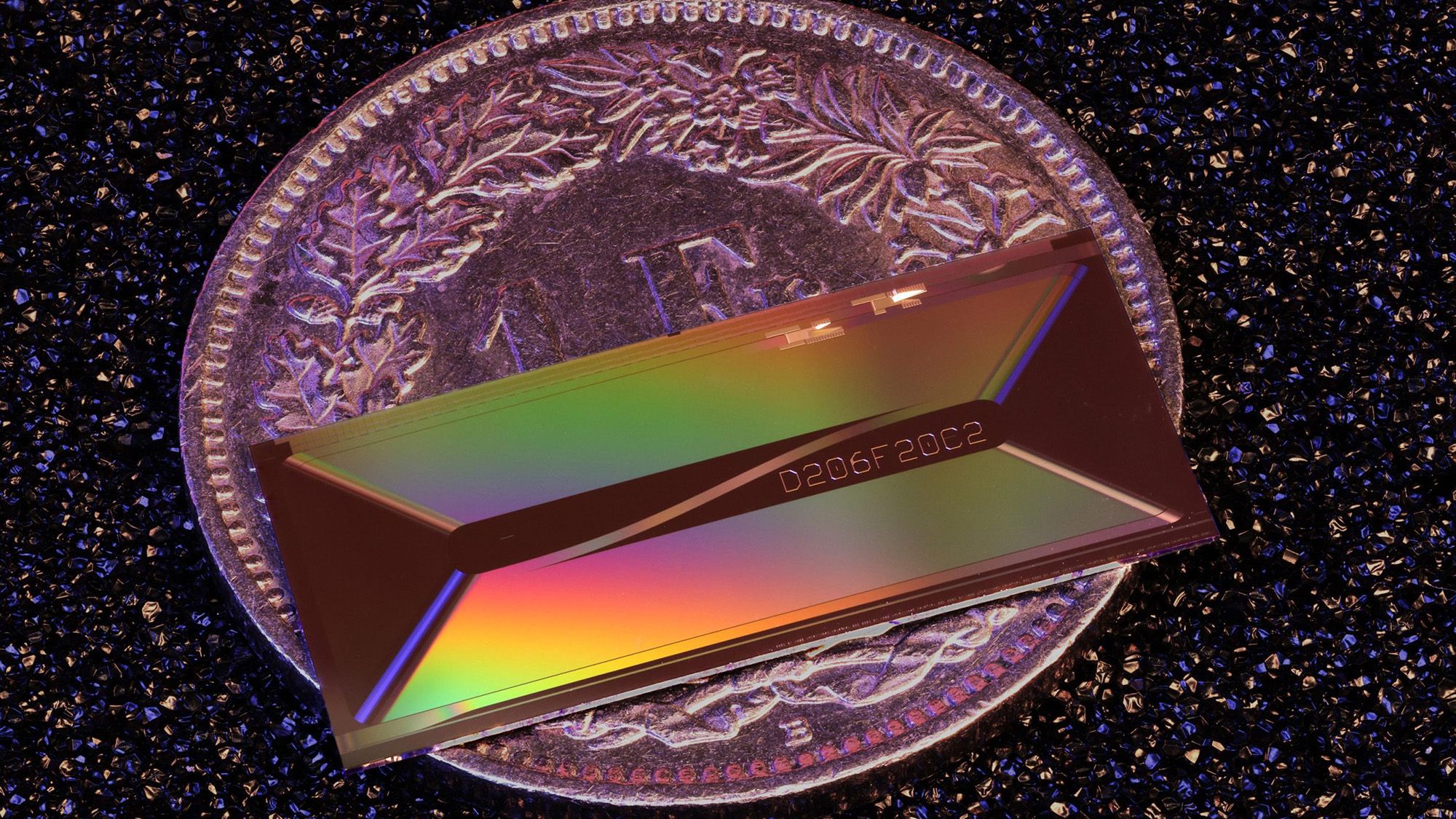
Researchers report that they have built an ultrafast laser on a tiny photonic chip and achieved output strong enough to compete with laboratory-class systems in some respects. According to the supplied source material, the device delivered pulses with 1.05 nanojoules of energy and a duration of 147 femtoseconds. In practical terms, that means extremely short, energetic bursts generated from a highly miniaturized platform.
The work addresses what Tobias Kippenberg of EPFL described as a “holy grail” of integrated photonics: producing a high-pulse-energy femtosecond laser on-chip. For more than two decades, that goal has remained stubbornly out of reach because the features that make ultrafast lasers powerful have also made them difficult to compress into chip-scale architectures.
Why ultrafast lasers are hard to miniaturize
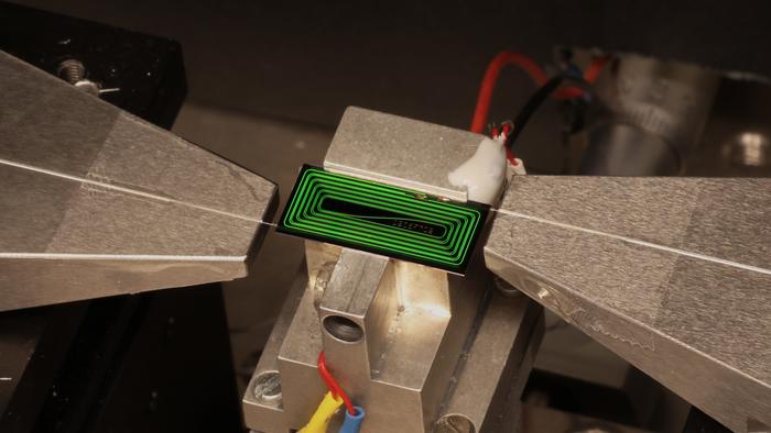
Photonic chips use light rather than electricity to carry and process signals. They do that through microscopic structures such as waveguides and resonant cavities. The approach is attractive because photonics can enable very high speed, low-loss signal handling, and compact optical systems. But fitting an ultrafast laser onto a chip is not as simple as scaling down a conventional design.
These lasers must produce intense pulses without destabilizing the system. Large laboratory setups have traditionally had more room to manage energy, heat, timing, and optical path design. On-chip platforms impose strict constraints on size and geometry, and those limits have made it difficult to achieve pulse energies high enough for demanding real-world applications.

The reported breakthrough came from revisiting an older laser architecture that the researchers say the integrated-photonics field had largely overlooked. The source text does not provide a full technical breakdown of every design element, but it makes clear that the team’s advance was not just about better fabrication. It was also about choosing a system architecture capable of supporting high-performance pulse generation within the confines of a chip.

Performance that changes the conversation
The numbers matter because they move chip-based ultrafast lasers closer to practical utility. A pulse duration of 147 femtoseconds means the light burst lasts only 147 quadrillionths of a second. At those timescales, ultrafast lasers can probe delicate physical and biological processes, cut or modify materials with extraordinary precision, and serve as timing references in advanced instruments.
Meanwhile, pulse energy above one nanojoule is significant in a field where miniaturized systems often sacrifice output strength for compactness. If a chip-based device can produce energetic pulses rather than merely short ones, it becomes much more relevant to diagnostics, imaging, and information-processing systems that currently depend on bulkier hardware.
The claim in the source text is not that the chip instantly replaces every tabletop ultrafast laser. That would overstate the result. Instead, the significance is that on-chip performance is beginning to enter a range where previously lab-bound capabilities could plausibly migrate into smaller, cheaper, and more deployable instruments.
Why that could matter across industries
If ultrafast lasers become chip-scale components, the immediate effect may be on portability and cost. Today, many systems that rely on these lasers require controlled lab or factory environments, not only because of the laser itself but because of the supporting optics and alignment demands. A photonic-chip implementation could reduce some of that complexity and enable more integrated products.
That creates obvious possibilities for medical diagnostics and imaging. Instruments that currently depend on specialized facilities could become smaller and more widely distributed. Manufacturing systems could benefit from more compact precision-light sources. Information-processing applications, including advanced optical timing and potentially some quantum or sensing platforms, could also gain from lasers that are both fast and integrated.
The broader industrial implication is familiar from the history of electronics: once a capability becomes chip-compatible, experimentation and commercialization tend to accelerate. Engineers can design around a standardizable part rather than a custom optical bench. That does not guarantee rapid mass adoption, but it usually lowers the threshold for product development.

An old idea, newly useful
One of the more revealing aspects of the report is that the breakthrough relied on a decades-old architecture that had been underappreciated. That is a reminder that not every frontier advance comes from inventing an entirely new principle. Sometimes progress depends on finding the right context for an older concept and combining it with modern fabrication, materials, and system-level insight.
In photonics, where design constraints can steer entire fields toward particular architectures, overlooked options can remain dormant for years. The researchers’ success suggests that some assumptions about what was practical on-chip may have been too conservative, or at least too tied to the dominant design playbook.
What comes next
The most important next question is not whether the result is impressive, but whether it can be engineered into repeatable devices that survive outside the lab. For chip photonics, manufacturability, stability, packaging, and compatibility with surrounding systems are what separate a strong paper from a platform technology.
Still, the direction is clear. This work pushes ultrafast photonics closer to the point where compact devices can do jobs once reserved for room-scale optical setups. That could expand access to high-end measurement and imaging tools in the same way earlier semiconductor advances expanded access to computation.
- The study demonstrates an ultrafast laser on a photonic chip.
- Reported output reached 1.05 nanojoules with 147-femtosecond pulses.
- The design relies on a previously overlooked laser architecture.
- Potential applications include diagnostics, imaging, manufacturing, and information processing.
For now, the breakthrough is best understood as a threshold moment rather than a finished commercial product. But in a field where size has long been one of the main barriers to broader use, proving that an ultrafast laser can perform credibly on-chip is a consequential step. If follow-on work can translate the result into robust devices, photonic systems may become smaller, cheaper, and much more widely deployable.
This article is based on reporting by Live Science. Read the original article.

Originally published on livescience.com