A new approach to stacking silicon is targeting one of chipmaking’s hardest tradeoffs
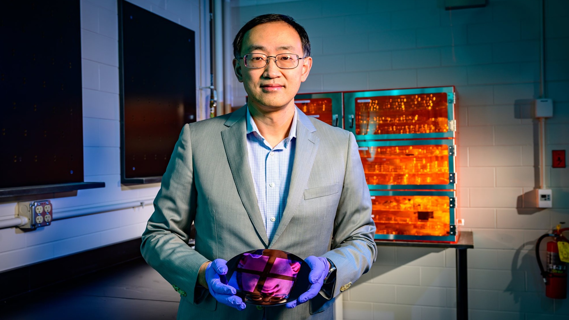
A research team at the University of Illinois Urbana-Champaign says it has developed a way to build monolithic 3D silicon chips at low temperatures while achieving near-perfect yields. If the result holds up through broader validation and scaling work, it would mark a notable step in the long-running effort to keep improving chip performance and density without relying only on traditional two-dimensional shrinking.
The core idea is significant because monolithic 3D integration has been discussed for years as a way to extend the useful life of silicon manufacturing. Instead of spreading more transistors across a flatter surface, engineers stack device layers more tightly on top of one another. In principle, that can reduce interconnect distances, improve bandwidth between functions, and open room for more capability in the same footprint.
The practical barrier has been process compatibility. High-performance silicon fabrication usually depends on thermal budgets that can damage or disrupt circuitry already built underneath. That is why the low-temperature element in this report matters. A process that allows additional layers to be added without undoing the performance of existing layers addresses one of the main reasons monolithic 3D designs have been difficult to industrialize.
Why yield is the headline number
The other standout claim is yield. In semiconductor manufacturing, ambitious process ideas often fail not because they cannot work once, but because they cannot work consistently enough to justify production. Near-perfect yields, if reproducible, imply that the researchers are not only showing a laboratory proof of concept but also moving toward the reliability threshold that determines whether a technique is commercially relevant.
That does not mean a direct jump to mass production is imminent. Research milestones and factory adoption sit on different timelines, and moving from a university process flow to full-scale manufacturing typically requires years of refinement, equipment work, and integration testing. Even so, yield data matters because it signals whether an idea is fundamentally fragile or potentially manufacturable.
For the broader industry, that distinction is crucial. As conventional transistor scaling becomes harder and more expensive, the next gains are increasingly expected to come from packaging, advanced memory, chiplet architectures, and new forms of vertical integration. A credible low-temperature monolithic 3D method would fit squarely into that mix.

What this could change in real systems
If the process can be extended beyond the laboratory, stacked silicon built under gentler thermal conditions could give designers more flexibility in how they partition logic, memory, and specialized accelerators. That matters in markets where moving data is often as costly as processing it. Bringing compute blocks closer together through dense vertical stacking could improve efficiency and performance at the same time.
It could also influence how manufacturers think about system integration. Today, many advanced products solve scaling limits by placing multiple dies in one package. That approach has delivered major gains, but it still comes with packaging complexity and interconnect overhead. Monolithic 3D integration offers a different promise: tighter coupling within the silicon itself rather than across separate chips.
Whether that becomes a complement to chiplets or a competitor to them will depend on cost, defect rates, power behavior, and the range of devices the process can support. Those answers are not contained in the initial summary, but the research result is notable because it speaks directly to one of the industry’s biggest structural questions: how to keep improving computing hardware when older versions of Moore’s Law become harder to sustain.
A research milestone worth watching closely
The University of Illinois Urbana-Champaign team is positioning its result at the intersection of performance, manufacturability, and thermal control. That is a strategically important combination. Plenty of semiconductor breakthroughs offer higher performance in isolation; fewer claim compatibility with the realities of fabrication.
For now, the prudent reading is that this is an important research signal rather than a finished production roadmap. Still, low-temperature monolithic 3D silicon with near-perfect yields is exactly the kind of result the industry has been waiting to see from academic labs. It suggests that vertical silicon integration may be moving from a compelling idea toward a more credible engineering path.
In a field where incremental gains increasingly require major technical compromises, that alone makes the work consequential. The next question is not whether stacked silicon is desirable. It is whether this approach can be repeated, generalized, and transferred into the manufacturing ecosystems that define modern computing.
This article is based on reporting by Interesting Engineering. Read the original article.
Originally published on interestingengineering.com