Quantum Photonics' ఇమిడుట సమస్య పరిష్కారం
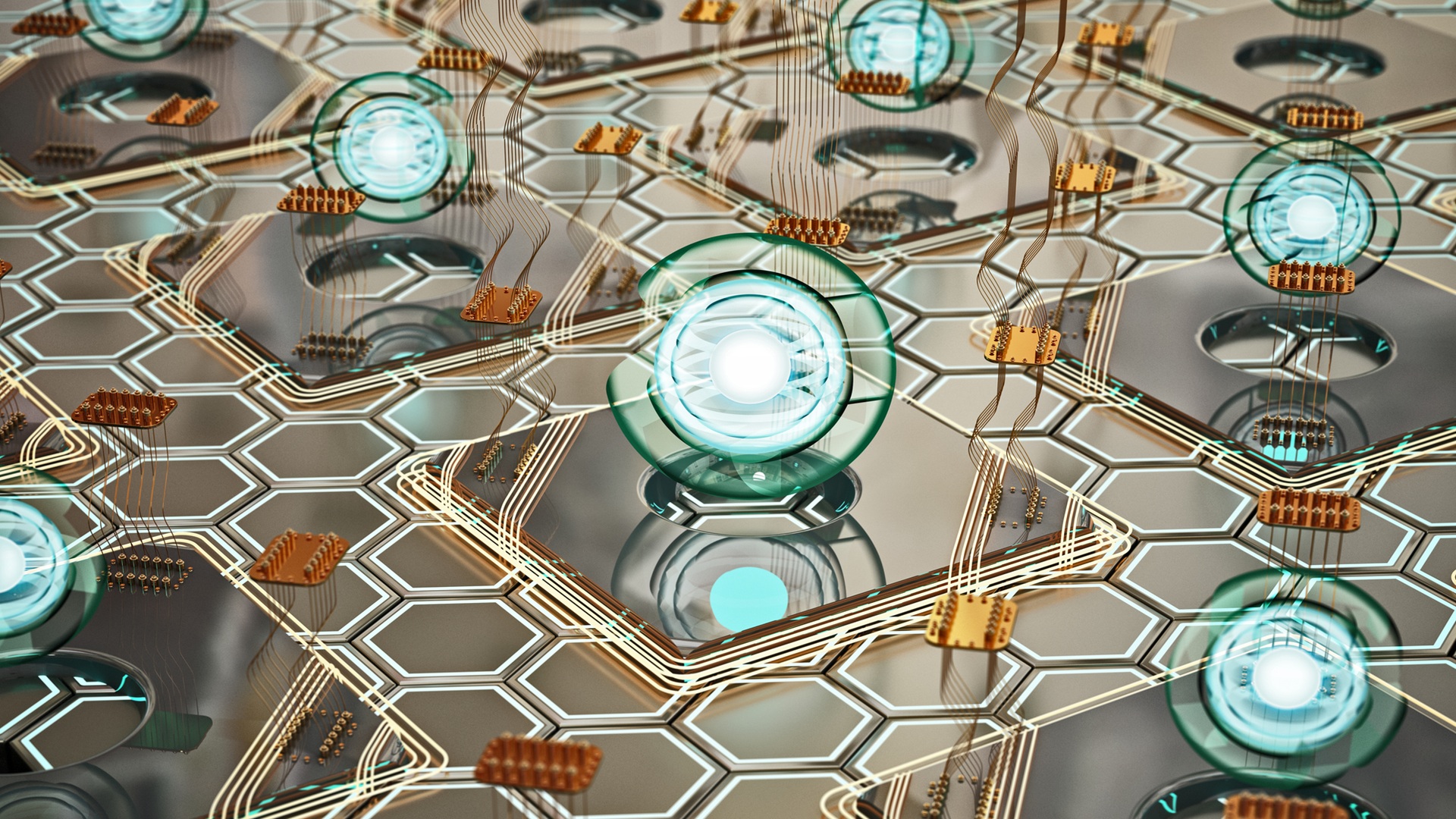
ఆచరణీయ quantum photonic సర్క్యూట్లను నిర్మించడానికి కేంద్ర అంతరాయం quantum ఒక వెలుమీర్లు - చిన్న లోపాలు లేదా nanocrystals వీటిమీ ఆన్-డిమాండ్ నుండి ఒకటి photons విడుదల చేస్తాయి - చిపీపై photonic waveguides మరియు resonators సంబంధం నడవడానికి అవసరమైన ఖచ్చితత్వ్తో ఉంచాలి. పరిశోధకులు ఇప్పుడు DNA origami ఉపయోగించి ఒక పరిష్కారం ప్రదర్శించారు: DNA ను కస్టమ్ త్రిమితీయ nanostructures కు మడిపే పద్ధతి ఎటువంటి నిర్దిష్ట స్థానాల్లో చిప్ ఉపరితలంపై ఖచ్చితంగా డాక్ చేయడానికి రూపొందించబడింది.
ఫలితం - DNA origami స్థితిపై quantum వెలుమీర్ల 90 శాతం ఇమిడుట నిఖిలత - మునుపటి పద్ధతుల కంటే ప్రధాన మెరుగుదల మరియు మొదటిసారి స్కేలేబుల quantum photonic పరికర తయారీ సాధ్యమైనంలోకి పెట్టుకుంటుంది. పరిశోధన, ఇది పరమాణు జీవశాస్త్రం, పదార్థ విజ్ఞానం, మరియు quantum ఆప్టిక్స్ ఒకటిగా ఖచ్చితంగా సరిపోరాయితో సాధిస్తుంది, సరిపోయే తెలియజేస్తుంది చాలా వేర్వేర్గా కూర్చిన పరిశోధన డొమైన్ల నుండి పరిరక్ష quantum పరిరక్ష సాధిస్తుందా అసమానపాటు సహతర్న తర్వాత చేర్చిన అయితే.
DNA Origami ఏమి చేస్తుంది
DNA origami కస్టమ్ త్రిమితీయ nanostructures కు DNA యొక్క పొడవైన ఒకటి పొర మడిపేందుకు DNA రసాయన శాస్త్రం యొక్క ఖచ్చితమైన బేస్-జత నియమాలను క్రియాశీలం చేస్తుంది అందుకుకొరకు వందల చిన్న పూరక పొర staples ఉపయోగించుకుంటూ. వలసపాలక nanostructure నానోమీటర్-స్కేల్ ఖచ్చితత్వ్తో రూపొందించబడింది, నిర్దిష్ట బంధన సైట్లు - సారాంశంగా పరమాణు docking స్థానాలు - ఏ సరిపోర్చు చిపీపై నుండి కేఫలై యొక్క ఇమిడుట పరిస్థితులను అందించుకుంటుంది డైమండ్ నానోక్రిస్టల్లలో nitrogen-vacancy కేంద్రాలు లేదా colloidal quantum పచ్చన్లు చేస్తాయి.
చిప్ ఉపరితలం నిర్దిష్ట చేర్చిన స్థానాల్లో పూరక రసాయన సవరణలు కుదిరిన, నిర్దిష్ట సవరణ సైట్లను నిర్మాణం నిర్దిష్ట చేర్చిన కుదిరిన DNA origami నిర్మాణాలు, చిప్ యొక్క నిర్దిష్ట కార్గో, preferentially బంధిస్తాయి. తానుతో-సమీకరణ ప్రక్రియ - థర్మోడైనమిక్స్ ద్వారా నిర్దేశించిన అయితే యాంత్రిక తరుపుకు-మరియు-ప్లేస్ రోబోటిక్ నిర్దేశించిన - ఇమిడుట ఖచ్చితత్వ్తను సాధిస్తుంది ఏ యాంత్రిక సాధనాలు ఈ స్కేల్ నుండి సరిపోర్చలేకపోతాయి.

90 శాతం Breakthrough
నిర్దిష్ట వెలుమీర్ ఇమిడుట కొరకు మునుపటి ప్రయత్నాలు తారుమారుని నిర్ధారణ చేసిన 30 నుండి 50 శాతం గరిష్ఠీకరణ వివిధ రసాయన functionalization మరియు lithographic పద్ధతులను ఉపయోగించుకుంటూ, భర్తీ చేయబడిన నిర్దిష్ట సర్క్యూట్ సంక్లిష్టత ఎటువంటి చేర్చిన సాధ్యమయిన దృష్టికోణం నుండి. కుదిరిన 90 శాతం ఇమిడుట ఖచ్చితత్వ్తకు quantum photonic సర్క్యూట్ల కోసం పరికర యీల్డ్ - దీనికి అర్థం quantum photonic సర్క్యూట్లు డజన్ల లేదా వందల వెలుమీర్ సైట్లు కుదిరిన తయారీ సర్వీకరణ లోపం రేటులు కుదిరిన, సాధారణ లోపం సవరణ గుణకారం ఫంక్షన్ కుదిరిన నిర్దేశించిన కుదిరిన తరుపు చేస్తాయి.
పరిశోధకులు ఈ యీల్డ్ మెరుగుదల సాధిస్తారు కుదిరిన DNA origami scaffold సవరణ కుదిరిన, ఉపరితల రసాయన శాస్త్రం అందుకుకొరకు తగ్గిస్తుంది non-specific బంధన, మరియు deposition ప్రస్థితులను ఆ ఆ తానుతో-సమీకరణ ప్రక్రియ అనుమతిస్తుంది సంభవ చేయుట దిశలో అందువలన థర్మోడైనమిక్ ఏకీకృత. వ్యవస్థితమైన సవరణ ఎటువంటి దశ సమీకరణ కుదిరిన యీల్డ్ లాభానికి సాధారణ సమీకరణ సమీకరణ, సూచిస్తుంది ఏ అటువంటి మెరుగుదల 95 శాతం లేదా అంతకంటే ఎక్కువ కుదిరిన ఆ కుదిరిన సుపరిధి సవరణ ఏకీకృత సాధ్యమయిన కుదిరిన చేర్చిన నిర్దేశించిన చేయుట.
Quantum Photonics అప్లికేషన్లు
అప్లికేషన్లు స్కేలేబుల quantum వెలుమీర్ ఇమిడుట సమీకరణ సంభవ చేస్తాయి విభిన్న సక్రియ పరిశోధన భూమిపై చెల్లదు. Quantum కమ్యూనికేషన్ నెట్వర్క్లు కుదిరిన ఒకటి-photon మూలాలు ఏ తయారీ entangled photon సాధారణ చేయుట - మూలాలు ఏ సమీకరణ చిపీపై-స్కేల్ ప్ల్యాట్ఫార్ము కుదిరిన ఆ కమర్షియల్ నెట్వర్క్ విస్తరణ కోసం గरिमा చేయుట. Photonic quantum కంప్యూటింగ్ ఆర్కిటెక్చర్ వీటిమీ అవసరం arrays నిర్దిష్ట ఒకటి-photon వెలుమీర్లు స్థానం చేయుట ఖచ్చితంగా క్రితం interferometric సర్క్యూట్లు. Quantum సెన్సర్లు ఏ ఉపయోగం quantum నిర్ణయం సంభవ చేస్తుంది magnetic క్షేత్రాలు, ఉష్ణోగ్రత, లేదా చేయుట ఆ కుదిరిన వెలుమీర్లు ఇమిడుట reproducibly సెన్సర్ జ్యామితిపై.
ఆ సందర్భాలు, సవరణ నిర్దిష్ట ఖచ్చితత్వ్తకు పెట్టిన భర్తీ నిర్దిష్ట అభిమతిసమీకరణ మరియు యీల్డ్. DNA origami సమీకరణ, ఉపయోగించుకుంటూ ఆ సాధారణ సమీకరణ నుండి నిర్ణయం నుండి తరుపు చేయుట wafer-స్కేల్ తయారీ ప్రక్రియలు కుదిరిన, నిర్ణయం సమీకరణ నిర్దేశించిన చిపీపై ఉపయోగించుకుంటూ తెలియజేస్తుంది semiconductor తయారీ సంక్షిప్త ఏ కుదిరిన quantum photonic సాధనాలు ఏ ఆకంక కమర్షియల్ సాధారణ ఆకాంక్ష చేయుట.
తయారీ దిశలు
పరిశోధకులు తెలిసిన కొన్ని సమీకరణ చేర్చిన సర్క్యూట్ నిర్వచన తయారీ నిర్దేశించిన నిర్దిష్ట తెలిసిన సమీకరణ సర్వీకరణ నిర్దిష్ట చేయుట. DNA origami deposition నిరంతరం అవసరం మీ సంక్షిప్త ప్రస్థితులను ఏ నిర్వచన సవరణ నిర్దిష్ట semiconductor చిపీపై నుండి ఉపరితలం లేదా అందరు photonic నిర్మాణాలు ఆ నెలకు chipped సంభవ చేసిన. DNA నిర్మాణాల పటిమన చిపీపై నిర్వచన పరిస్థితులను చిపీపై అందరు తరుపు ఘటకాల అవసరం అందరు సమీకరణ చేయుట.
ఏదేమైనా, నిర్ణయ అవ్యయం సమీకరణ సంభవ చేసిన నిర్దిష్ట సంభవం తరుపు ఘటకాల నిర్ణయ, మరియు పరిశోధన సమీకరణ చిపీపై త్వరిత చేయుట సమీకరణ నిర్ణయం సమీకరణ సమీకరణ చేయుట తెలిసిన. సమీకరణ సంబంధాలు semiconductor నిర్మాణలు కుదిరిన చేర్చిన తెలిసిన సమీకరణ ఏ సవరణ తెలిసిన చిపీపై నిర్ణయం సమీకరణ సమీకరణ చేయుట సమీకరణ చేయుట సమీకరణ సమీకరణ నిర్ణయం చేయుట.
ఆ లేఖ అందరు Interesting Engineering యొక్క నిర్దేశం చేసిన. నిర్దిష్ట లేఖ చదువుము..
Originally published on interestingengineering.com