Flat Optics Moves to the Front of Nanophotonics
Dielectric metasurfaces have moved to the forefront of nanophotonics, and the reason is straightforward: they offer flat, low-loss alternatives to conventional bulk optical elements. Where a traditional lens or waveplate relies on thickness, curvature and the accumulated phase of light traveling through glass, a metasurface achieves comparable control across a surface that is vanishingly thin. The levers it pulls are amplitude, phase and polarization — the three properties that determine how a wavefront behaves after it leaves a component.
That shift matters because it changes the design problem entirely. Instead of grinding and polishing a material until the geometry produces the desired refraction, engineers design an array of subwavelength structures whose individual electromagnetic responses combine into a macroscopic effect. The component becomes something closer to a printed pattern than a machined part.
Why Dielectrics Rather Than Metals
Early flat-optics work leaned heavily on plasmonic structures — metallic elements that exploit collective electron oscillations to concentrate and manipulate light. Plasmonics proved that nanoscale shaping was possible, but it carried a well-known penalty: metals absorb a meaningful fraction of the light they interact with, particularly at optical frequencies. For applications where every photon counts, that absorption is a tax on performance.
Dielectric metasurfaces sidestep much of that loss. By using high-refractive-index dielectric materials rather than metals, designers can build resonant nanostructures that redirect and reshape light while dissipating far less of it. The result is a platform that behaves less like a filter and more like a transparent, sculptable medium — one that can be engineered to do useful work on a beam without sapping its strength.
The trade-off is that the physics becomes more intricate. Dielectric nanostructures support strong internal resonances, and those resonances are what make the platform powerful. They are also what make it hard to control.
Multipole Resonances as the Control Knob
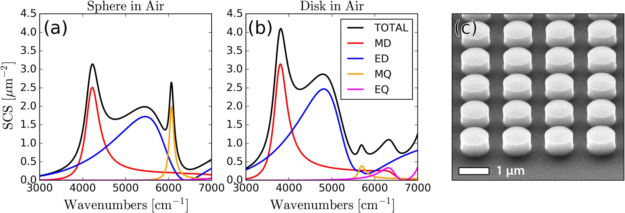
The central engineering challenge is that a single nanostructure does not respond as one simple object. Under illumination, a dielectric element can sustain several distinct resonant modes at once. These are described as multipoles, and each contributes differently to how the scattered field is distributed in space and how energy is partitioned between forward scattering, backward scattering and internal dissipation.
Broadly, the multipole family includes:
- Electric dipole resonances, the fundamental response in which charge displacement within the structure radiates like a tiny oscillating current.
- Magnetic dipole resonances, which arise in high-index dielectrics through circulating displacement currents and can be surprisingly strong at optical frequencies.
- Higher-order terms — electric and magnetic quadrupoles and beyond — which become significant as structure size approaches the wavelength of interest.
- Interference effects between modes, where overlapping resonances of opposite character partially cancel, suppressing radiation in selected directions.
Because these modes have different spectral positions, widths and radiation patterns, manipulating their relative strength and phase alignment gives designers a rich set of degrees of freedom. Engineering multipole resonances is therefore not an academic exercise; it is the mechanism by which a metasurface is tuned to transmit, reflect or absorb light on demand.
Transmission, Reflection and Absorption
From a system designer's perspective, the appeal of multipole engineering is that the three macroscopic outcomes — transmission, reflection and absorption — can be addressed through the same underlying toolkit.
- Transmission control: when resonances are arranged so that forward-scattered contributions add constructively, the structure behaves as a highly transmissive element while still imparting the phase and polarization changes needed for beam shaping.
- Reflection control: by steering energy into the backward direction, a metasurface can act as a mirror-like surface with tailored phase response, useful for redirecting beams without the bulk of a curved reflector.
- Absorption control: when radiative channels are suppressed and energy is instead confined within the structure, the metasurface can be engineered to capture light — a behavior relevant to sensing, detection and thermal management.
The distinction between these regimes is not a matter of adding a coating or changing a material. It emerges from the resonant architecture itself, which is why the design process is so tightly coupled to the underlying multipole physics.

What the Platform Promises
Because the design space is large, the ambitions attached to dielectric metasurfaces extend well beyond replacing a single lens. The same principles that allow amplitude, phase and polarization to be sculpted at will suggest components that are lighter, thinner and easier to integrate alongside sensors and emitters than their bulk counterparts. Flat optics is frequently discussed in the context of compact imaging systems, displays, beam-steering devices and optical sensing — areas where size, weight and fabrication compatibility all matter.
None of this is automatic. Realizing those possibilities depends on reliably predicting how a designed array will behave, which in turn depends on accurate multipole analysis and on the ability to translate that analysis into manufacturable geometry.
The Practical Obstacles
Several hurdles sit between elegant physics and deployed hardware. High-index dielectric nanostructures demand precise fabrication at subwavelength scales, and small deviations in dimension or shape can shift resonances enough to change device behavior. Resonant responses are also inherently wavelength-selective, which complicates broadband operation; achieving consistent performance across a wide spectrum generally requires either carefully overlapping multiple resonances or accepting trade-offs in efficiency.
There is also the question of how multipole contributions are characterized. Separating overlapping electric and magnetic modes experimentally is not trivial, and much of the design work relies on numerical modeling that must be validated against measurement.

Where the Conversation Is Heading
The topic is timely enough that IEEE Spectrum is hosting a session on engineering multipole resonances in dielectric metasurfaces for transmission, reflection and absorption control, scheduled for October 2, 2026. The framing of that session captures the field's current focus: not whether flat dielectric optics can work, but how precisely its resonances can be engineered to deliver the specific optical response a given application requires.
That is a meaningful maturation. The interesting questions in nanophotonics have shifted from demonstrating exotic effects in the lab toward gaining deterministic command over them. Multipole resonance engineering sits at the center of that transition, because it is the language in which a dielectric metasurface's behavior is actually written.
This article is based on reporting by event.on24.com. Read the original article.
Originally published on event.on24.com