A two-decade photonics goal may finally be within reach
Researchers at EPFL say they have built the first integrated ultrafast laser capable of matching the performance of traditional tabletop femtosecond lasers. Reported in Nature, the device produces pulse energies of 1.05 nanojoules and pulse durations as short as 147 femtoseconds directly from a photonic chip.
If those figures hold up as the technology moves outward from the lab, the achievement could mark a major turning point for integrated photonics. For more than twenty years, high-pulse-energy femtosecond lasers on chip were treated as a kind of holy grail: clearly valuable, theoretically possible, but stubbornly out of reach in practice.
Why ultrafast lasers matter
Ultrafast lasers are essential tools across modern optics because they generate extremely short pulses of light. Those pulses enable high-precision applications in manufacturing, surgery, spectroscopy and frequency-comb systems, including the optical atomic clocks that underpin the most accurate timekeeping technologies in existence.
The problem has been size and cost. Conventional femtosecond systems often occupy large optical tables and require complex alignments and specialized environments. That has limited where they can be deployed and who can realistically use them.
A chip-scale equivalent changes that equation. If powerful ultrafast lasers can be fabricated and integrated more like photonic components in telecommunications hardware, the technology could become smaller, cheaper and more accessible.

The overlooked architecture that made it work
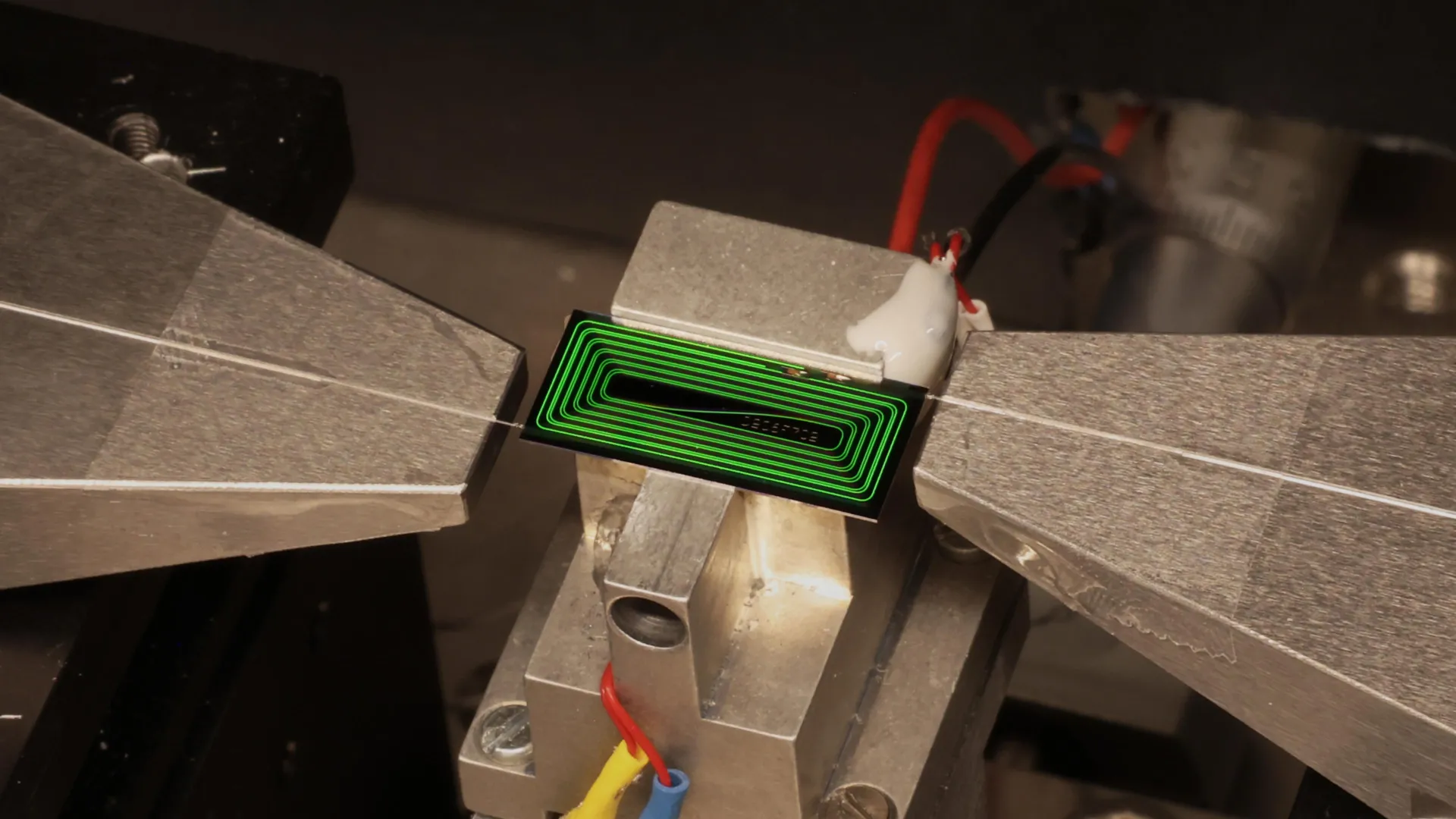
According to the supplied source text, the EPFL team led by Tobias J. Kippenberg adopted a Mamyshev oscillator architecture, a design that had received relatively little attention in integrated photonics. The system places a nonlinear waveguide between two optical filters that pass different parts of the spectrum. As an intense pulse travels through the waveguide, its spectrum broadens, allowing the filters to shape and stabilize ultrafast pulse formation.
The importance of that choice is not just that it worked, but that it suggests the barrier was not purely material or manufacturing-related. Sometimes a long-standing problem remains unsolved because the field is looking in the wrong design space. The EPFL result implies that integrated photonics may have overlooked a particularly effective route to high-energy femtosecond operation.
Kippenberg described the chip-based result as something the field had regarded as a “holy grail.” That language reflects how central the challenge has been. Many photonic technologies have shrunk successfully onto chips, but ultrafast, high-energy pulse generation remained one of the hardest to translate.
What this could unlock
The potential applications named in the supplied material span medical diagnostics to atomic clocks. Those examples hint at a broader consequence: when a high-performance optical tool becomes chip-scale, it can move from specialized research infrastructure toward deployable systems.
That matters in at least three ways. First, compactness lowers the barrier to integration into instruments that cannot accommodate table-sized lasers. Second, manufacturability can reduce cost and improve reproducibility. Third, on-chip compatibility creates the possibility of combining ultrafast light generation with other photonic functions in more tightly integrated devices.
In practice, that could affect sensing, communications, precision measurement and portable scientific instrumentation. Not every tabletop system will disappear, but the range of environments where femtosecond-grade performance is available could expand sharply.
A milestone for integrated photonics
Photonic chips already play a major role in telecommunications, where waveguides direct light much as electronic circuits direct current. Extending that miniaturization logic to ultrafast laser generation has been an obvious ambition, but obvious ambitions are often the hardest ones to realize because they require performance, not just convenience.
The EPFL team’s claim is important precisely because it is not just about fitting a laser onto a chip. It is about doing so while matching the performance of established femtosecond systems. That distinction separates a useful demo from a potentially field-changing platform.
There is still a difference between a landmark paper and a mass-deployed product. Packaging, reliability, manufacturing yield and system integration will all matter next. But the result reported here suggests the long effort to compress one of optics’ most powerful tools into a chip-scale format has crossed a meaningful threshold.
Why this stands out
- The device reportedly achieves 1.05 nanojoules of pulse energy and 147-femtosecond pulses on chip.
- The work appears in Nature and targets a long-standing goal in integrated photonics.
- The team used a Mamyshev oscillator architecture that had been largely overlooked for this purpose.
- Potential applications include diagnostics, precision metrology and optical clock systems.
This article is based on reporting by Science Daily. Read the original article.
Originally published on sciencedaily.com